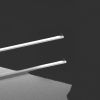
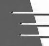
Conductive AFM Probes
Pt coated, DPE (low-noise) and DPER (high-res) AFM Probes
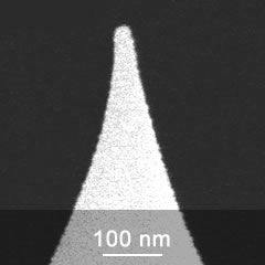
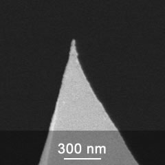
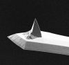
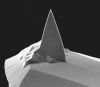
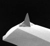
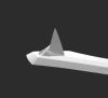
The pyramidal silicon etched AFM probes with an overall conductive platinum coating are suitable for a wide range of electrical AFM applications. The platinum coating is a 30nm thick film on both sides of the AFM cantilever.
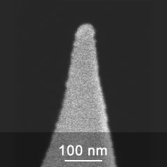
The special DPE AFM probes feature silicon AFM tips with a stack of conductive layers, which provides a more stable electrical signal and less noise. Because of the increased AFM tip radius, some reduction of resolution in the topography image is possible when using DPE AFM probes in comparison with the regular platinum coated AFM probes.
The special DPER AFM probes are made by depositing a thin platinum coating on silicon AFM tips. While the thickness of the coating on a flat AFM cantilever surface is about 15nm, there is only a 10nm increase in the AFM tip dimensions compared to bare silicon AFM probes.
Typical radius of uncoated AFM tip
8nm
Resulting AFM tip radius with the coating
<30nm (Pt coated)
<40nm (DPE)
<20nm (DPER)
Full AFM tip cone angle*
40°
Total AFM tip height
12-18µm
AFM Probe material
n-type silicon
AFM Tip coating
Platinum
Detector coating
Platinum
*The full cone angle may be less than 40° at the last 200nm of the AFM tip end.
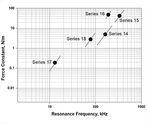
1 AFM Cantilevers Series
| AFM Cantilever | Resonance Frequency, kHz | Force Constant, N/m | ||||
|---|---|---|---|---|---|---|
| min | typical | max | min | typical | max | |
| 14 series | 110 | 160 | 220 | 1.8 | 5.0 | 13 |
| 15 series | 265 | 325 | 410 | 20 | 40 | 80 |
| 16 series | 170 | 190 | 210 | 30 | 45 | 70 |
| 17 series | 10 | 13 | 17 | 0.06 | 0.18 | 0.40 |
| 18 series | 60 | 75 | 90 | 1.2 | 2.8 | 5.5 |
3 AFM Cantilever Series
| AFM Cantilever | Resonance Frequency, kHz | Force Constant, N/m | |||||
|---|---|---|---|---|---|---|---|
| min | typical | max | min | typical | max | ||
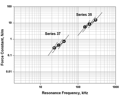
| 35 series | Cantilever A | 130 | 205 | 290 | 2.7 | 8.9 | 24 |
| Cantilever B | 185 | 300 | 430 | 4.8 | 16 | 44 | |
| Cantilever C | 95 | 150 | 205 | 1.7 | 5.4 | 14 | |
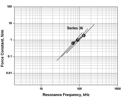
| 36 series | Cantilever A | 30 | 90 | 160 | 0.1 | 1.0 | 4.6 |
| Cantilever B | 45 | 130 | 240 | 0.2 | 2 | 9 | |
| Cantilever C | 25 | 65 | 115 | 0.06 | 0.6 | 2.7 | |
| 37 series | Cantilever A | 30 | 40 | 55 | 0.3 | 0.8 | 2 |
| Cantilever B | 15 | 20 | 30 | 0.1 | 0.3 | 0.6 | |
| Cantilever C | 20 | 30 | 40 | 0.1 | 0.4 | 1 | |
4 AFM Cantilever Series
| AFM Cantilever | Resonance Frequency, kHz | Force Constant, N/m | |||||
|---|---|---|---|---|---|---|---|
| min | typical | max | min | typical | max | ||
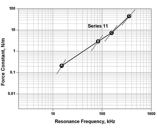
| 11 series | Cantilever A | 12 | 15 | 18 | 0.1 | 0.2 | 0.4 |
| Cantilever B | 60 | 80 | 100 | 1.1 | 2.7 | 5.6 | |
| Cantilever C | 115 | 155 | 200 | 3 | 7 | 16 | |
| Cantilever D | 250 | 350 | 465 | 17 | 42 | 90 | |
Application of Pt coated AFM probes
The electric properties of different materials can be mapped to the topography images using AFM probes with conductive coatings, when AC or DC bias is applied between the AFM tip and the sample. Contact mode or two-pass operation technique can be used for this purpose. The data can be used for analysis of the structure and composition of heterogeneous samples as well as for quantitative characterization of individual grains or defects on surface.
Though silicon is conducting in bulk due to the presence of the dopants, the surface of the AFM probe is always coated by a thin (1-2nm) native oxide film. That is why using the conductivity of uncoated silicon AFM probes for AFM measurements is possible only in UHV conditions after the oxide film is removed. For imaging the electric properties of materials in ambient conditions, AFM probes with special conducting coatings are usually used.
Platinum coated AFM probes are comonly used for Electrostatic Force Microscopy (EFM) and Kelvin Probe Force Microscopy (KPFM) investigation.
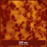
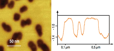
Height and phase images of the rubber-modified isotactic polypropylene filled with carbon black. The images were obtained in Electric Force Microscopy mode using HQ:NSC14/Pt AFM probes. Images courtesy of S. Magonov (Bruker).
Application of HQ:DPE-XSC11
DPE AFM probes have increased coating thickness, which gives more freedom for using them in contact electrical modes. The AFM probes provide better performance and higher contrast of electrical signals, while the ability to resolve the small surface details might be reduced. The AFM probes can be used in electric AC modes when a study of the electric properties of a sample has higher priority. This is demonstrated in AM-FM images of a fluoroalkane layer.
Among the serious limitations of Electrical Force Microscopy are the sensitivity and signal-to-noise ratio. Enlargement of the AFM tip radius leads to a loss of resolution in both topography and EFM imaging, while it does not always reduce the noise in the maps of electric properties.
DPE AFM probes offer a special structure of conductive layers applied to the AFM tip that improves signal-to-noise ratio with little impact on the resolution.
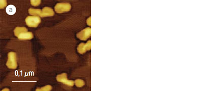
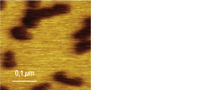
Topography, surface potential and dC/dz scans of a fluoroalkane (F12H20) on a silicon substrate are presented in Fig. 1. below. As you see the resolution in topography image made using a standard platinum coated AFM probe (a) is better because the 6.5nm lamellar structures are clearly resolved and the shape of brighter features is not as rounded as in the image made with the DPE AFM probe (b). Still, the better signal-to-noise peformance is provided by the DPE AFM probe (d,f). Topography image, Pt coated probe") (a) Topography image, Pt coated AFM probe
(a) Topography image, Pt coated AFM probe
 Topography image, DPE probe") (b) Topography image, DPE AFM probe
(b) Topography image, DPE AFM probe
 Surface potential map and cross-section, Pt coated probe") (c) Surface potential map
(c) Surface potential map
and cross-section, Pt coated AFM probe
 Surface potential map <br />and cross-section, DPE probe") (d) Surface potential map
(d) Surface potential map
and cross-section, DPE AFM probe
 dC/dz map and cross-section, Pt coated probe") (c) dC/dz map and cross-section,
(c) dC/dz map and cross-section,
Pt coated AFM probe
 dC/dz map and cross-section, DPE probe") (d) dC/dz map and cross-section,
(d) dC/dz map and cross-section,
DPE AFM probe
Comparison of AM-FM scans (5kHz-10kHz) of a fluoroalkane layer made using a regular Pt coated AFM probe and a DPE AFM probe. Scan size 350nm. The DPE AFM probe provides better signal-to-noise performance, while the topography resolution is better with the Pt-coated AFM probe. Images courtesy of Sergei Magonov, Agilent Technologies (Agilent 5500 AFM).
![]() Detailed specifications of HQ:DPE-XSC11 »
Detailed specifications of HQ:DPE-XSC11 »
Application of HQ:DPER-XSC11
The DPER AFM probes are made by depositing a thin contonuous Pt coating on silicon AFM tips. While the thickness of the coating on the flat AFM cantilever surface is about 15nm, there is only a 10nm increase of the AFM tip dimensions compared to the bare silicon AFM tips, resulting in an AFM tip radius below 20nm.
The DPER AFM probes can be used for imaging samples with high lateral resolution. Due to the thin coating, the electrical signal may be noisy. One should also not expect coating stability in contact or hard tapping regimes of AFM operation.
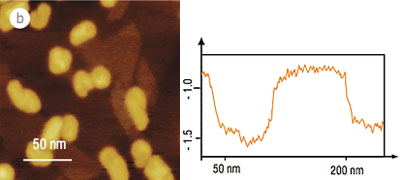
Single-pass KPFM scans of semifluorinated alkane (F14H20) deposited on graphite. The shape of brighter features in the scan made with a DPER AFM probe (a) is not as rounded as in the image made with the thicker Pt coated AFM tip (b). In addition to self-assembled structures on the top, the lamellar structures with 6.3nm spacing can be clearly seen in the underlying layer in DPER image (a). Still the better signal-to-noise peformance in surface potential images cannot be achieved with DPER AFM probe (a) in comparison to (b). Images courtesy of Sergei Magonov, Agilent Technologies (Agilent 5500 AFM).
Videos
-
Products
-
HQ:NSC18/Pt
-
- 75 kHz 2.8 N/m
-

-

-

-
-
HQ:NSC35/Pt
-
- 205/300/150 kHz 8.9/16/5.4 N/m
-

-
-
-
-
HQ:DMD-XSC11
-
- 18/110/210/450 kHz 0.5/6.5/18/95 N/m
-

-
-

-
-

-

-
-
HQ:NSC36/Pt
-
- 90/130/65 kHz 1.0/2.0/0.6 N/m
-
-
-
-
-
HQ:DPER-XSC11
-
- 15/80/155/350 kHz 0.2/2.7/7.0/42 N/m
-
-
-
-
-
-
-
HQ:DPE-XSC11
-
- 15/80/155/350 kHz 0.2/2.7/7.0/42 N/m
-
-
-
-
-
-
-
HQ:NSC15/Pt
-
- 325 kHz 40 N/m
-
-
-
-
-
HQ:NSC16/Pt
-
- 190 kHz 45 N/m
-
-
-
-
-
HQ:NSC14/Pt
-
- 160 kHz 5.0 N/m
-
-
-
-
-
HQ:XSC11/Pt
-
- 15/80/155/350 kHz 0.2/2.7/7.0/42 N/m
-
-
-
-
-
-
-
HQ:CSC37/Pt
-
- 40/20/30 kHz 0.8/0.3/0.4 N/m
-

-
-
-
-
HQ:CSC17/Pt
-
- 13 kHz 0.18 N/m
-
-
-
-