There are many AFM applications where the scan size exceeds 10µm while characteristic size of the surface features is larger than 30nm. For these applications, the lateral resolution is of less importance compared to other characteristics of AFM probes such as mechanical durability and ability of contamination. Furthermore, many AFM applications require blunt AFM tips to allow quantitative measurements of various physical properties of the sample (friction, indentation, adhesion).
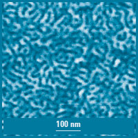
| Fig. 1. Height image of polystyrene-polybutadiene-polystyrene triblock copolymer. Scan obtained in tapping mode using a hardened AFM tip with radius about 30nm. Image courtesy of S. Magonov (Bruker). |
 |
Contact mode
Hardened AFM probes offer larger tip-sample contact area resulting in higher loads exerted to sample. However, these AFM probes can still be used in contact mode on hard samples.
Contact electric techniques may require AFM cantilevers with higher spring constants than in regular contact mode (up to 50N/m). Relatively soft (0.03-0.3N/m) conducting AFM cantilevers are optimal for higher lateral resolution. AFM cantilevers with higher force constant are better for quantitative measurements. Platinum coated AFM probes are not recommended for contact mode electric techniques. Conductive diamond coated HQ:DMD series AFM probes can handle much better the combined mechanical stress and elevated temperatures at the tip-sample contact area in applications such as Conductive AFM and Tunneling Current AFM.
Tapping mode
The choice of probes with hardened DLC coated AFM tips (series HARD) with a radius of <20nm is reasonable for routine surface investigations of large surface areas (>10µm) with surface features larger than 20nm in size. Here, HARD AFM probes provide resolution comparable to standard AFM probes and Hi'Res-C AFM probes. HARD AFM probes also allow long-term experiments due to the enhanced mechanical durability.
For imaging in liquids, AFM probes with a chemically stable Cr-Au coating can be used. The AFM tip radius with a coating on the AFM tip side is below 35nm.
To image electric properties of materials using two-pass techniques, AFM probes with conducting coatings are needed. The coatings may increase the AFM probe tip radius up to ~40nm depending on the selected series. Pt coated AFM probes with an AFM tip radius <30nm offer the best compromise between resolution and durability.
The AFM tip radius with Co-Cr magnetic coating is below 60nm. As the size of magnetic domains is usually more than 50nm, such an AFM tip radius is enough for MFM.
