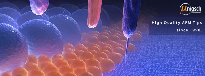
AFM Tips
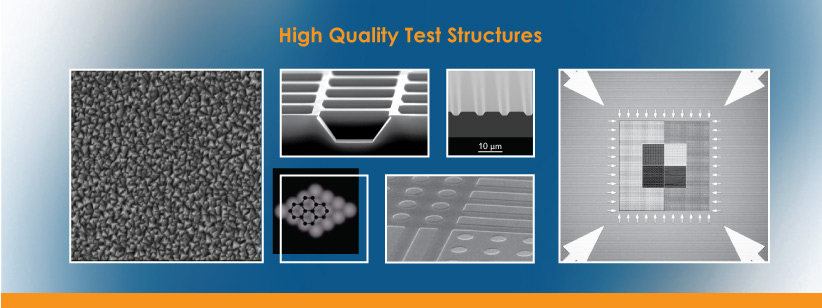
Test structures
Resources
Contacts
Search
Login
Cart
MikroMasch Catalog
EN
CN
Prices
+359 2 865 86 29
info@mikromasch.com
MikroMasch AFM Tips • World's Most Trusted Value Brand
Tapping Mode AFM Probes
Soft Tapping Mode AFM Probes
Contact Mode AFM Probes
High Resolution AFM Probes
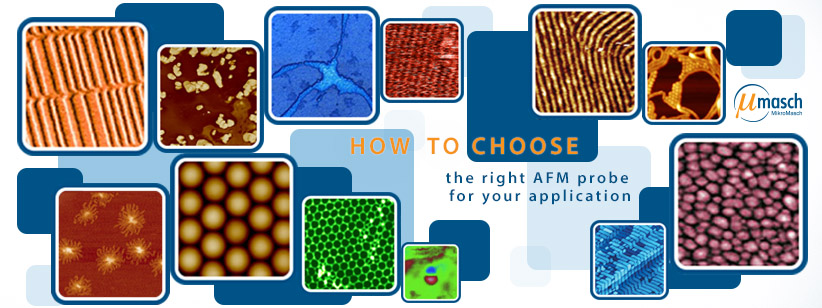
Life Science / Bio AFM Probes
Conductive AFM Probes
Diamond AFM Probes
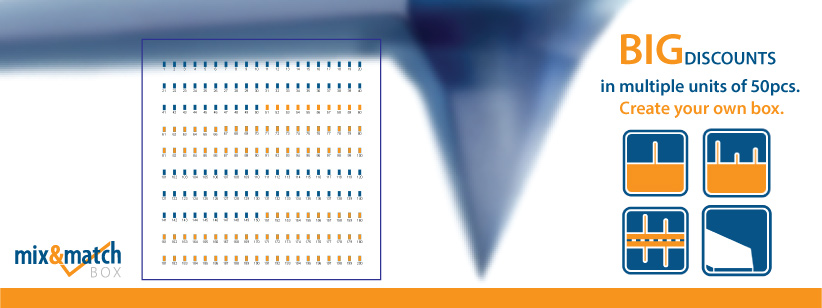
Mix & Match Box
X
-
 MikroMasch Catalog