AFM was introduced as a contact mode technique, in which the quasistatic deflections of the AFM cantilever caused by tip-sample interactions were used for a feedback-control surface imaging. The AFM tip engagement is followed by rastering it over a sample surface in a way that the tip-sample force was kept at the set-point level by adjusting the vertical sample (or AFM tip) position. In this way, a piezoelectric scanner pivots the AFM tip precisely along the surface profile.
In further AFM developments, oscillatory modes were introduced, in part, to avoid shearing sample deformation in contact mode. In these modes, a piezoelement positioned close to the AFM probe is used to excite the AFM cantilever oscillation at its resonance frequency. As the oscillating AFM probe approaches a sample and comes into intermittent contact with it, the oscillation parameters such as amplitude, frequency, phase, quality factors are changing. Amplitude modulation and frequency modulation, in which respectively the AFM cantilever amplitude or frequency (phase) are chosen for feedback during scanning, are the main AFM oscillatory modes.
The contact and oscillatory modes have a large number of related techniques that were developed in response to different characterization needs. Besides surface imaging performed in the contact and oscillatory modes, there are spectroscopic modes based on measurements of deflection, amplitude, or phase changes as the AFM probe approaches a sample and retracts from it. These curves (often named 'force curves') can be measured at a particular location or when obtained at multiple locations can be combined into maps (also known as 'force volume').

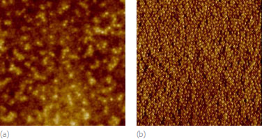
Fig. 1. Height (a) and phase (b) images of block copolymer (polystyrene-block-poly-4-vinylpyridine) film obtained in Tapping Mode using HQ:NSC16 AFM probes. Scan size 500nm. Image courtesy of Dr. Sergei Magonov.
Initially, AFM probes were made by gluing a diamond shard to an AFM cantilever cut out of metallic foil or by tapering a Fe, Ni or W wire. This tedious preparation has been substituted later by batch production of AFM probes using semiconductor technologies. In the first commercial AFM probes the AFM cantilever and AFM tip consisted of a thin Si3N4 film on a glass substrate. The AFM tip has a square pyramid shape with a nominal radius of curvature at the AFM tip apex ~20nm. According to the preparation technology these AFM probes can be made thin, which defines relatively small spring constants in the 0.01-0.6N/m range. These AFM probes are regularly used for imaging in contact mode and applied to soft samples.
The AFM tip shape and radius at the apex are important parameters that define the range of applications and the quality of the probe. Large surface corrugations limit lateral image resolution substantially and bring the AFM tip shape into the play. For imaging of critical-dimension structures such as deep and narrow trenches, specially etched AFM probes (for example, with a FIB technology) or those made of carbon nanotubes or Hi'Res-C spikes should be used. High-resolution imaging of flat samples depends primarily on the AFM tip apex.
Monolithic silicon AFM probes, which are etched from a Si wafer, are most appropriate for ambient and vacuum AFM studies. Their AFM cantilevers have a rectangular shape with the following parameters: width 30-60µm, length 100-400µm, thickness 1-8µm. Force constants of commercial AFM probes vary in the 0.01-600N/m range. Typical dimensions of silicon AFM tips are: height 8-20µm, opening angle of ca. 30-40°, apex radius 10nm. They have a pyramidal shape, which in the ideal case should be triangular near the apex.
Silicon AFM probes are sharper than Si3N4 ones, yet they have limitations in stiffness when imaging soft samples is of interest. An appropriate solution for high-resolution imaging of such objects can be obtained by making hybrid AFM probes consisting of Si3N4 AFM cantilevers and silicon AFM tips. Unfortunately, such AFM probes are rare.
In addition to sharp AFM probes, which are applied for high-resolution imaging, there is sometimes a need for AFM probes with large apex dimensions. AFM probes with rounded apex shape with a diameter in the 50-100nm range are in demand for nanomechanical measurements and also for low-wear imaging.
Characterization of AFM probes is rather important issue because variations in the AFM tip shape and apex size are not uncommon. There are direct and indirect ways of characterization of the AFM probes. Scanning electron microscopy (SEM) and transmission electron microscopy (TEM) provide a direct visualization of the tip AFM shape and apex dimensions. The indirect experimental procedure is based on imaging special test structures such as nanoporous Al. The analysis of the images obtained on such test samples helps determining the shape of the tip and its apex size. The test samples should be used with extreme caution by performing probe evaluation in the low-force regime in order to avoid tip damage.
Al back side coating improves the reflection of the laser beam. In some cases, a researcher sacrifices reflectivity in order to avoid a possible bending of the cantilever in experiments at different temperatures. There is also a chance that the coating of the cantilever backside brings some additional material to the probe apex thus making it duller.
For measurements of the electric or magnetic properties of samples the AFM cantilever coatings play the most essential role. These studies require coated probes with different stiffness as well as with apexes of various sizes. The silicon AFM probes in our catalog are available with a number of coatings.
Further reading
Contact mode
Non-contact mode
Tapping mode
