Contact Mode
High resolution PFM imaging
Conductive AFM probes with low force constant
HQ:CSC17/Pt
Quantitative PFM measurements
Conductive AFM probes with medium force constant
HQ:NSC18/Pt
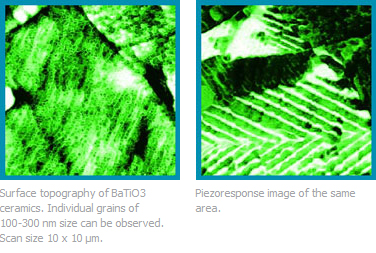
Progress in electronic devices based on ferroelectric heterostructures requires an understanding of the local ferroelectric properties at the nanometer level. SPM is one of the most promising techniques that allows local property measurements. Using SPM, one can image and modify local domain structure, perform quantitative characterization of individual grains in ferroelectric thin films and analyze the dependence of the hysteresis loop parameters on the grain crystallographic orientation [1].
| Fig. 1. Images courtesy of Sergei V. Kalinin, Tony Alvarez, Dawn A. Bonnell, University of Pennsylvania. |
 |
Among the SPM techniques, the most widely used for ferroelectric imaging is currently piezoresponse force microscopy (PFM). This technique is based on the detection of electromechanical surface oscillations due to the inverse piezoelectric effect induced by the AC bias on the AFM tip. Spectroscopic modification of PFM allows local electromechanical hysteresis loops to be obtained. PFM can also be used for modification of the local domain structure on the nanometer level by applying a DC bias to the AFM tip.
Relatively soft (0.03-0.3N/m) conductive AFM cantilevers are optimal for high lateral resolution (~7-10nm). Stiff AFM cantilevers (1-50N/m) are required for quantitative measurements of hysteresis loops.
1) S. V. Kalinin, A. Gruverman, D. A. Bonnel, Appl. Phys. Lett., 85, 794 (2004)
Contact Mode
High resolution PFM imaging
Conductive AFM probes with low force constant
HQ:CSC17/Pt
Quantitative PFM measurements
Conductive AFM probes with medium force constant
HQ:NSC18/Pt