Tapping Mode
Roughness measurements of flat or corrugated surfaces
Hi'Res-C AFM probes with medium force constant
Hi'Res-C14/Cr-Au
The ability of an AFM probe to profile sub-micron structures is important for a number of technological applications in the semiconductor and data storage industries. With the shrinking dimensions of semiconductor and storage devices, it is becoming more and more difficult to find suitable techniques for quality control. Atomic Force Microscopy (AFM) can be used for such a function, but its limitations have to be considered for accurate application.
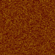
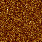
This issue is easily observed in studies of the surface roughness of silicon wafers and the porosity of low-K materials. As the sharpness of the AFM tip increases, finer surface features can be revealed which leads to a larger effective roughness estimated from height images. This effect is illustrated by two images of a silicon wafer, one obtained with a standard HQ:NSC14 AFM probe and the other obtained with a high resolution Hi'Res-C14 AFM probe. The two height images are compared below in Fig. 1a-b.
| Fig.1. AFM images of a silicon wafer surface from a standard silicon AFM probe (left) and a Hi'Res-C AFM probe (right). Scan size 1µm. Dimension 5000 AFM. Images courtesy of Dr. S. Magonov (Agilent). | |
 |
 |
| L 17.578nm RMS 0.145nm 1c DC Ra(1c) 0.034nm Rmax 0.114nm Rz 0.114nm Rz Cnt 2 SL 17.586nm HL 17.578nm VD 0.436nm Angle 1.422° |
L 15.625nm RMS 0.324nm 1c DC Ra(1c) 0.123nm Rmax 0.421nm Rz 0.421nm Rz Cnt 2 SL 15.684nm HL 15.625nm VD 0.868nm Angle 3.179° |
Not surprisingly, the roughness determined with the high resolution AFM probe is larger than the roughness determined with the regular AFM probe. Knowing that there are large quantitative differences from using different AFM tips, it is important to clarify what type of data is necessary for your application. If a qualitative comparison of the roughness of similar samples is needed, a regular AFM tip may be sufficient. However, if accurate quantitative roughness data is needed, it may be necessary to use a Hi'Res-C AFM tip for the best possible results.
It is worth noting that measurements taken with a sharp AFM tip require special precautions (a gentle engagement procedure and low-force imaging) to avoid the unnecessary damage of the AFM tip. Please refer to the High Resolution page for details).
Tapping Mode
Roughness measurements of flat or corrugated surfaces
Hi'Res-C AFM probes with medium force constant
Hi'Res-C14/Cr-Au