The technique of local anodic oxidation (LAO) is used for writing very small oxide patterns on both metallic and semiconductor surfaces. Research groups worldwide employ this technique for the fabrication of nanoelectronic devices, nanoelectromechanical systems, electro-optical structures, and templates for chemical and biological self-assembly. Modern SPM equipment allows for direct writing on the surface in a very accurate and well-controlled manner.
The phenomenon of anodic nano-oxidation is electrochemical in nature. The simplified mechanism is as follows. A thin water film covering the surface under a controlled humidity of about 50% serves as an electrolyte between the sample (anode) and the tip (cathode). The negatively biased AFM tip imposes an external electric field which dissociates the water molecules, creating OH-. The field causes the OH- ions to drift away from the AFM tip towards the surface, where they react with surface atoms to form an oxide layer localized beneath the tip. The field strength decays across the growing oxide film and the oxide growth process self terminates at/below the critical electric field, which is on the order of 109V/m. The growth rate of the oxide is strongly dependent on the bias applied to the AFM tip. The oxide grows in both vertical directions relative to the surface of the sample, the depth growing slightly more quickly than the height.
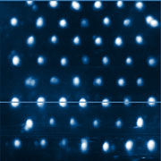
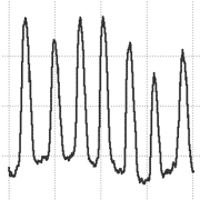
Fig. 1a shows the AFM height image of a Ti film with ordered points of local oxidation (the oxide islands are about 10nm in diameter). Fig. 1b shows the surface profile along the blue line. Platinum coated AFM probes with C~20N/m were used for LAO, while the height images were obtained in tapping mode using an HQ:NSC15 AFM probe.
| Fig.1. Ti film with ordered islands of dielectric oxide obtained by high-resolution electric lithography. |
 |
 |
| (a) Height image. Scan size 200nm, Z-scale is 8nm. |
(b) Surface relief section profile along the dotted line. |
LAO requires the absence of a gap between the AFM tip and the surface, so the AFM tip must be able to sustain significant mechanical loads. AFM probes with relatively high force constants (5-50N/m) are recommended. Though silicon AFM probes are usually doped for technological reasons, there is a thin native oxide layer on the surface of Si that makes the AFM probes non-conducting. This is the reason why probes with special chemically inert coatings having low electromigration firmness are used in these experiments.
When using HQ:NSC14/Pt AFM probes for LAO, subsequent imaging of the oxidized pattern can be performed with the same AFM probe. However, an uncoated AFM tip might give better resolution of the oxide islands.

