Tapping Mode
Imaging of general shape and estimation of average dimensions
HQ:NSC AFM probes with medium force constant
HQ:NSC14/Al BS
Imaging of the single fibers
Hi'Res-C AFM probes with medium force constant
Hi'Res-C14/Cr-Au
Molecular wires (sometimes called molecular nanowires) are molecular-scale objects which conduct electrical current. They are the fundamental building blocks for molecular electronic devices. Their typical diameters are less than three nanometers, while their lengths may be macroscopic, extending to centimeters or more.
Unlike the more familiar nanowires (which are crystals), molecular nanowires are composed of repeating molecular units, which may be organic (e.g. DNA) or inorganic (e.g. Mo6S9-xIx). Molecular nanowires often aggregate in solution into bundles.
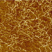
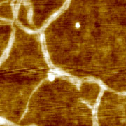
Fig. 1 presents images of triphenylene molecules spincast from hexane onto a Si/SiO2 substrate. A very low concentration solution was used to get a submonolayer. The molecules stack to form fibers due to strong pi-pi interactions between benzenes in the core to form molecular wires. Image (b) obtained using a Hi'Res-C AFM probe clearly shows the organic fibers packed together, whereas for the General Purpose AFM probe only one big fiber can be seen.
| Fig. 1. Images of triphenylene molecules spincast from hexane onto Si/SiO2 substrate. The molecules form fibers due to strong pi-pi interactions between benzenes in the core. Bioscope with Nanoscope IIIa controller from Digital Instruments. Images courtesy of Thuc-Quyen Thai Nguyen. |
|
 |
 |
| (a) Image obtained using a standard HQ:NSC14 AFM probe. Scan size 2µm. | (b) Image obtained using a high resolution Hi'Res-C14/Cr-Au AFM probe. Scan size 300nm. |
Molecular-scale objects are delicate samples that require very gentle imaging conditions in tapping mode due to their small size and weak adhesion to the substrate. General shape and average dimensions of the particles can be acquired using General Purpose AFM tips with curvature radius of 10nm. Imaging soft delicate samples requires soft AFM cantilevers.
When fine features need to be resolved, one should use Hi'Res-C probes on the same AFM cantilevers for further reduction of tip-sample interaction forces and geometrical dilation effects. When using Hi'Res-C "light tapping" conditions are preferable, which implies low resonance amplitude (start at 0.2V up to 1.2V) and a set point ratio of about 0.9 to 1. Scan rate should start at below 1Hz. Scan size should start out at 50nm (250nm maximum). See the High Resolution page for details.
Tapping Mode
Imaging of general shape and estimation of average dimensions
HQ:NSC AFM probes with medium force constant
HQ:NSC14/Al BS
Imaging of the single fibers
Hi'Res-C AFM probes with medium force constant
Hi'Res-C14/Cr-Au