AFM Probes and AFM Cantilevers
An AFM cantilever with an AFM tip on its end is the main sensing component ultimately responsible for the quality of AFM imaging. The most common and at the same time very sensible scheme of data acquisition is an optical one based on registration of a laser beam reflected from the backside of the AFM cantilever with a sectioned (position sensitive) photodiode. For better reflection the backside of AFM cantilevers is often covered with aluminium or gold. There are a number of other deflection registration techniques and related peculiarities of AFM cantilever construction among which piezo cantilevers are worth of particular consideration [160, 161, 210, 211, 390, 921, 922, 1382]. However, this report is limited to the description of AFM cantilevers for the optical registration scheme.
AFM cantilever parameters
- Material of the AFM cantilever
The most popular materials are monocrystalline silicon and Si3N4. Silicon nitride AFM cantilevers offer an advantage over silicon ones in the sense that they may be produced thinner and, hence, more flexible (having lower stiffness). However, Si3N4 does not possess perfect manufacturability for AFM tips machining, therefore Si3N4 AFM tips are usually inferior to those made of silicon. The merits of both materials have been coupled together in hybrid AFM probe construction, which features the flexibility of a silicon nitride AFM cantilever and the sharpness of a silicon AFM tip [1442].
AFM cantilevers made of tungsten, nickel and another materials are in occasionally used [157, 581, 602, 870, 921, 922, 943, 1022, 1065, 1328]. The material through its inherent mechanical properties (elasticity module or Young's module E, module of rigidity G) and density defines the stiffness, resonance frequency and Q-factor (see below) of the AFM cantilever. In addition, the material properties of the coating should also be taken into consideration if it covers over the entire AFM cantilever surface.
Using AFM cantilevers made of low resistance materials such as metals or highly doped silicon ensures that no electrostatic charges collect at the AFM tip apex. Gathering electrostatic charges results in distortion of the images and is especially crucial in Scanning Tunneling and Electrical Force Microscopy studies.
- Geometry of the AFM cantilever
A number of AFM cantilever geometries have been proposed since the invention of AFM and even earlier when Scanning Tunneling Microscopy was the only SPM technique of comparable principle of operation. The most preferable among researchers are the rectangular (diving board) and the triangular lever shapes. Triangular AFM cantilevers are often used in such contact mode experiments where twisting a tip along the only symmetry axis of the lever is undesirable. The range of geometries of the AFM cantilevers manufactured by MikroMasch is wide:
| AFM Cantilever Property |
Range for MikroMasch AFM cantilevers |
Range of AFM cantilevers from reviewed publications |
| Length (l) | 90µm - 450µm | > 10µm |
| Width (w) | 13.5µm - 50µm | > 3µm |
| Thickness (s) | 500nm - 7µm | > 0.1µm |
| Force constant (k) | 0.03N/m - 45N/m | 0.001N/m - 400N/m |
| Resonance frequency (fo) | 10kHz - 450kHz | 3kHz ~ 10Mhz |
- Stiffness of the AFM cantilever
Stiffness is defined by the force constant k measured in N/m (or sometimes nN/nm). The commonly used AFM cantilevers have force constants in the range 0.01-100N/m. The "soft" AFM cantilevers with k<0.1N/m are chosen mainly when using contact mode in order to affect the sample to minimal extent. The rigid ones with k>1N/m are often used in non-contact or dynamic modes since they exhibit high resonance frequencies and small oscillation amplitudes of about several tens Angström. This ensured wide dynamic frequency range and substantially raises sensitivity.
 |
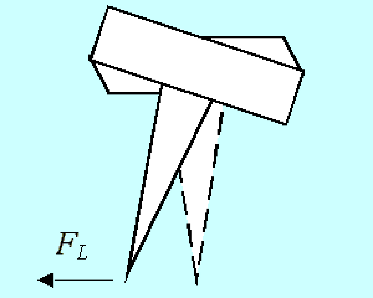 |
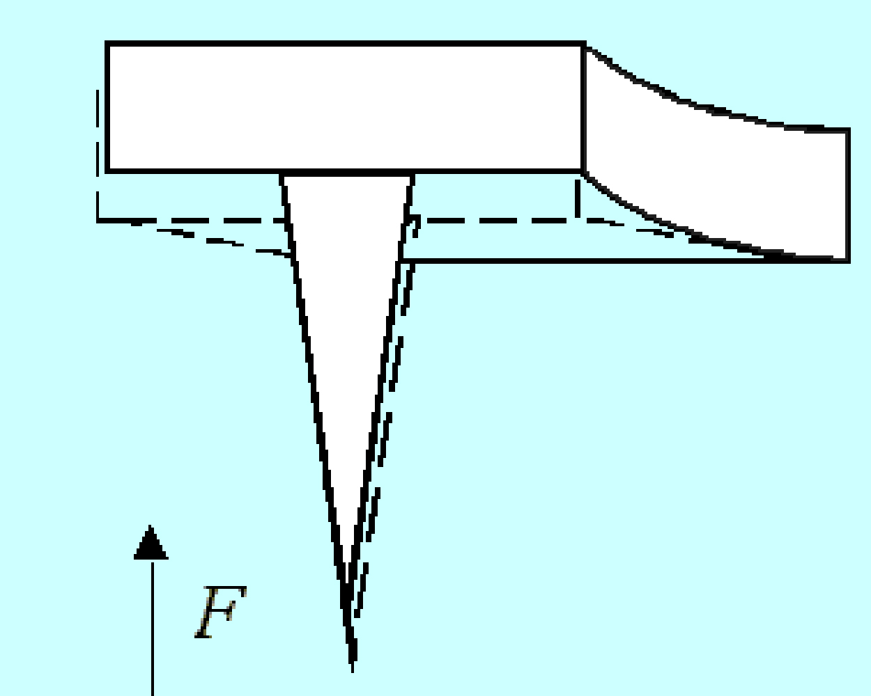
| Fig. 1.1 Schematic of vertical deflection | Fig. 1.2 Schematic of lateral deflection |
By default the term "force constant" refers to the force constant with respect to vertical deflection of the AFM cantilever (Fig.1.1). The theoretical expression for estimation of this force constant in the case of the simplest rectangular AFM cantilever is given by following formula:
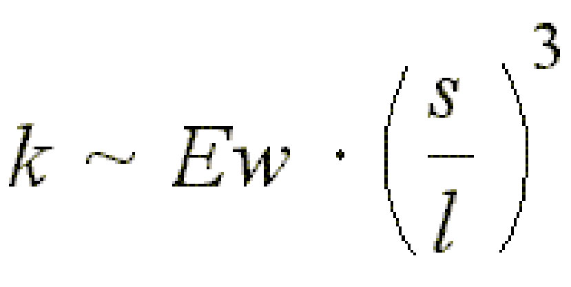
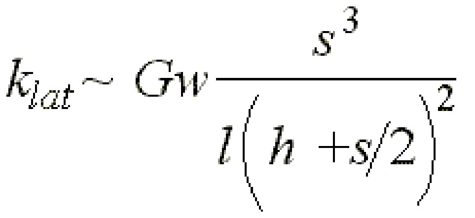
In a number of SPM techniques especially in Lateral Force Microscopy (LFM) the tip is moved in touch with the surface of the sample and twisting of the AFM cantilever apart from vertical deflection also takes place as depicted in Fig 1.2. The stiffness of the AFM cantilever from such kind of applied external force is determined by the lateral force constant, which can differ from that of "normal" k to a great extent. The formula for klat has the same structure except for an additional parameter h defining AFM tip height:
By additional processing of commercial AFM cantilevers Kageshima et al. [1437] enhance the lateral force sensitivity of Atomic Force Microscopy for detection of molecular scale interactions. Sensors of two types are fabricated by this group. As a result, the lateral force constants are reduced about 10-fold and 180-fold for both types respectivelly which allows for improvement of lateral force resolution up to 1nN.
The expressions for determination of the force constants of triangular levers are more complicated [1308]. See also a useful paper of Newmeister and Ducker [1218].
It is commonly adopted that triangular AFM cantilevers withstand much better lateral forces in comparison to rectangular ones of identical normal stiffness. Rigorous calculations performed by Sader [2622] show that the reality is quite the contrary. This unexpected theoretical result is to be verified experimentally.
It is a nontrivial task however to measure exactly the force constant of a particular AFM cantilever mainly due to the fact that geometrical parameters of every AFM cantilever cannot be exactly controlled and determined individually in mass production. Therefore, the theoretically calculated stiffness may substantially differ from the actual one. This concerns particularly the thickness control during the etching process of AFM cantilever micromachining. A simple calculation shows that the variation of thickness in ± 20 % results in variation of k value in the range of about -50%~+70%. To cope with this unsertainty a number of empiric and semiempiric techniques of force constant measuring and calibration are developed [E008, 859, 1300, 1205, 1206, 1621, 2626].
Determining the mechanical properties of materials at the micro and nanoscale needed for microprocessor design and development of micro-elecrtomechanical systems (MEMS) is a challenge due to the inadequate testing equipment since it must be capable of applying loads in the order of 10-6 to 10-9 Newtons. AFM with well-calibrated silicon AFM cantilevers is quite promising technique for such measurements. Comella and Scanlon [756] report on the development of AFM cantilever based technique for mesuring the elasticity of thin films. In their simple and reliable approach microcantilevers of the investigated material are formed by an ordinary lithographical method, then a silicon AFM cantilever with a well-calibrated force response is used to measure microbeams deflection under defined loadings. The authors claim that the method developed is applicable to beams of thickness ranging from Angströms to microns. Vice versa, using calibrated loading (for example, with an indenter) the unknown force constant of the AFM cantilever can be measured [E011].
Visit also the Materials Research section and subsections within for numerous examples of materials characterization.
- Resonance frequency of the AFM cantilever
Resonance frequency fo varies from several kHz up to several Mhz [163] and analytically is expressed as:
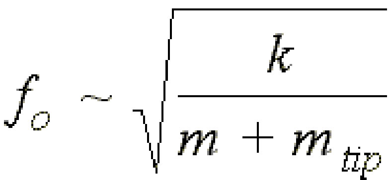
where m and mtip are masses of an AFM cantilever and an AFM tip respectively. In the simplest case of a rectangular AFM cantilever neglecting the AFM tip mass it is derived that:
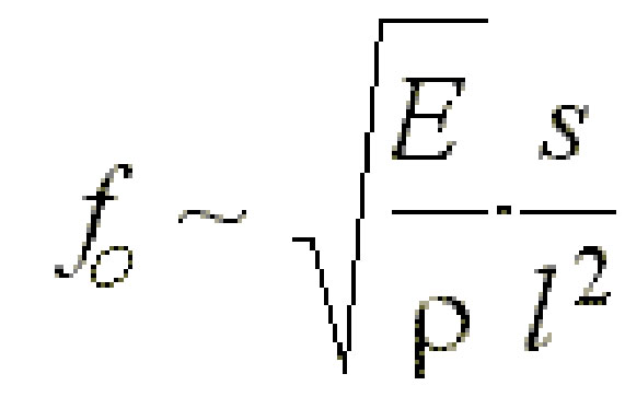
It can be easily seen that the decisive factor to increase the resonance frequency is to shorten the length of an AFM cantilever. At the same time the AFM cantilever can be produced relatively "soft" by means of width or thickness adjustments compensating the increase of the force constant due to appearance of l in the denominator of the expression for k. The AFM cantilevers with high resonance frequencies fo and low k are the better choice for tapping mode investigations since the AFM tip taps the surface gently while at the same time oscillates at several hundred kilohertz [519, 1578].
The eigenfrequency of the AFM cantilever can vary significantly if the latter is coated with a rather thick coating like, for instance, DLC. Salvadori at al [85] investigate the dependence of fo from the thickness of DLC coating deposited on the AFM cantilevers of 3.5 - 5 µm thicknesses using a specially derived formula for a thin and uniform coating with thickness s. This dependence is found to be almost linear. A 0.3 µm coating raises the eigenfrequency of the AFM cantilever by 50%. However, deposition of thick DLC films results in severe bending of the AFM cantilever as shown in photographs presented by Lemoine at al [82]. This bending originates from the intrinsic stress in DLC films. It can be released substantially by incorporating silicon atoms (~ 15 %) in a-C:H film. The authors note that stress-induced AFM cantilever deflections are too large for direct use of the AFM cantilevers in an AFM microscope. The bending gives rise to works on stress measurements in thin films grown on silicon cantilever beams ([1649]).
Fritz et al. [1211] report on the successful deposition of a thin copper film onto conductive silicon AFM cantilevers by MikroMasch produced by means of a galvanic displacement technique. This procedure does not lead to bending of the lever and keeps the resonance frequency almost unchanged. To demonstrate the effectiveness of this approach for tribological studies, the coated AFM cantilevers are chemically functionalized with alkanethiol monolayers. The effect of the changed surface energy is detected with adhesion measurements in water and ethanol.
- Q-factor
The Q-factor shows what part of the entire vibration energy that system loses during a full cycle of oscillation. In other words, it defines the minimal external vibration force within a given range of frequencies needed to maintain the oscillation of the system. Ideally, no external force is needed since it contributes to the overall noise thus reducing sensitivity. In highly damping ambients such as liquids substantial external forces are needed and therefore the Q-factor is smaller by 2 - 3 orders of magnitude than that in ultrahigh vacuum. In mechanical systems it is approximated as:
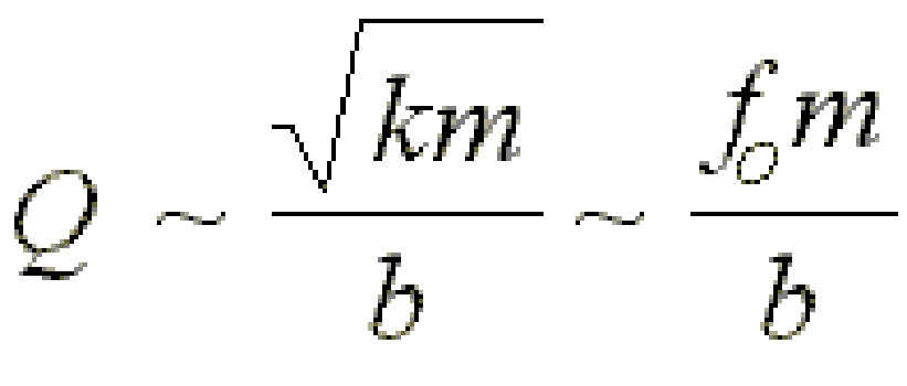
where b is the damping factor. Thus the Q-factor depends on the mechanical characteristics of the AFM cantilever and the damping properties of the ambient. The higher the Q-factor, the higher the sensitivity. See a publication on this topic by Yasumura et al. [1210].
AFM tip parameters
-
Material of the AFM tip
The choice of material depends on the purposes the AFM probe is intended for. When the highest possible hardness is necessary, for example in nanoscratching experiments or Scanning Spreading Resistance Microscopy (SSRM), a diamond AFM tip is glued to the AFM cantilever [602, 1606, 1609]. Another approach is to use a conventional silicon AFM tip with a diamond-like coating (DLC) [1336].
Resistance of the AFM tip and the entire AFM cantilever against aggressive ambients especially in the case of fluids is of primary importance as well. This problem is often solved using protective coatings such as Cr-Au or Pt.
The protective coatings at the same time can serve as conductive coatings. TiN, W2C, TiO, doped DLC and many others are occasionally used. AFM cantilevers with such tips are suitable for Scanning Tunneling Microscopy (STM), Electric Force Microscopy (EFM) and other conductance sensitive techniques. In principle, the silicon AFM tip itself can be used for such purposes if made of highly doped silicon. However, it is easily damaged in contact mode techniques such as the above mentioned SSRM where very high contact forces of 10-5 N are applied to the specimen [157].
Another class of coatings includes magnetic ones such as Co, Ni, Fe and a number of special alloys for use in Magnetic Force Microscopy (MFM) and Scanning Tunneling Microscopy investigations [642, 873, 1111, 1117, 1122, 1123, 1126, 1176, 1441]. The magnetic AFM probes by MikroMasch are listed here.
Since the mid 1990's a novel approach for functionalization of the AFM tip apex with other molecules in order to build specific AFM probes and sensors is developing intensively. Until now different micro-, macromolecules and functionalization addenda have been proposed and investigated as candidates for supertips: carbon nanotubes [30, 78, 818, 1325, 1380, 1381, 1456, 1464, 1610], W2C nanotubes [1445], proteins [974], adamantane [270], caltrop shaped molecules based on a differentially substituted tetrahedral silicon atom [E009] and many others [451, 1211, 1622]. Besides inherent extrasharpness the functionalized AFM tips possess selectivity with respect to the features on the sample surface having different chemical nature and are ideally suited to mapping their distribution and performing single-molecule force spectroscopy studies. Of course, to measure such tiny forces down to 10-12 N and gradients of 10-5 N/m very sensitive and intelligent registration and feedback systems are necessary.
Functionalization of the AFM tip apex with various agents allows for preferential imaging of different atoms at the sample surface. Ke et al. [13] investigate theoretically the effect of tip morphology on the image contrast for a GaAs(110) surface for the three atomically different AFM tip apexes of a Si tip: (1) Si apex with a half-filled dangling bond; (2) Ga apex with an empty dangling bond; and (3) As apex with a fully filled dangling bond. The study reveals a great impact of the dangling-bond states of different atoms at the tip apex on the image contrast. Calculation reveals that the Ga apex images the As sublattice, and the As apex images the Ga sublattice, and in the case of the Si apex, it is possible to image only the As sublattice or both the As and Ga sublattices, depending on the tip-sample separation.
- Geometrical parameters of the AFM tip
These are the height, profile, opening angle at the tip apex and apex curvature radius.
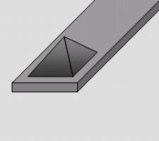
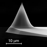
The overwhelming majority of former commercial AFM tips have triangular or square pyramid shape with an opening angle up to 70° (Fig. 2, a). They are produced by lithography and do not actually exhibit sufficient sharpness.
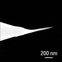
Using the (electro)chemical etching technique sharper AFM tips can be produced from monocrystalline silicon. The bulk shape of this AFM tip is still pyramidal and not so sharp (< 40°, Fig. 2, b) but the very end of the tip tends to become increasingly thinner approaching the apex. The opening angle near the apex is about 20°. Nevertheless, the pyramidal profile of the AFM tip does not still allow imaging of high aspect ratio structures.
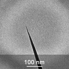
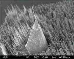
If high aspect ratio samples with steep and deep walls are to be investigated, long and thin AFM tips resembling a bee sting (Fig. 2, c) are used. Such AFM tips are grown on the apexes of the conventional AFM tips using Electron Beam Deposition (EBD). Other techniques such as Focused Ion Beam (FIB) machining [2594] or oriented growth of whisker-like silicon needles [1281] are also developed. The latest advances in technology of carbon nanotubes allow attachment or direct growth of carbon nanotubes as an extratip at the AFM tip apex of commercial AFM cantilevers (Fig. 2, e).
The resolution of Scanning Probe Microscopy depends substantially on the sharpness of the imaging AFM tip. Curvature radius of conventional AFM tips is about 8 - 15 nm. Very high resolution is achievable with Hi'Res-C AFM tips specially developed by MikroMasch (Fig. 2, d). Curvature radii of these AFM tips are in the order of 1 nm and with their help fine molecular or even atomic structure can be resolved.
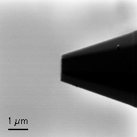
In some studies very specific AFM probe tips are required, for example AFM tips with a flat apex (Fig. 2, f). Such AFM tips are used in tribological, indentation and other studies.
 |
 |
 |
| a | b | c |
 |
 |
 |
| d | e | f |
| Fig. 2 AFM tip variety. (a) AFM probe with pyramidal AFM tip. (b) AFM probe with conventional silicon AFM tip. (c) AFM probe with EBD grown AFM tip. (d) SEM image of an old Hi'Res-C AFM tip. (e) AFM probe with Carbon Nanotube AFM tip. Image taken from [1612] with permission of Dr. R. Schlaf. (f) AFM probe with flat AFM tip apex. | ||
Sometimes there is no apparent dependence between AFM tip characteristics and imaging parameters. For example, Sedin and Rowlen [21] observe two different trends for measured surface roughness as a function of AFM tip size. Root mean squared (RMS) roughness is one of the most commonly reported measures of surface roughness from AFM images. It is found that at small lateral scan sizes (<500nm) the image root mean square roughness decreased as AFM tip size increased, but at larger scan sizes (e.g. 5000nm), the roughness increases with increasing AFM tip size. The authors also emphasize that there is a great variation of AFM tip shapes within a single lot of commercial AFM cantilevers. Frost et al. [27] show that AFM tip quality has a strong influence on the surface roughness parameters extracted from the AFM images particularly for surfaces with low surface roughness (~1nm) as generally obtained by means of thin film technologies. For evaluation of the influence of the actual AFM tip quality on the measured surface topography they propose nanometer-sized sputtered InP-structures whose sizes are well-controllable with a set of parameters of the sputtering process.
There are also attempts to estimate the effect of AFM tip apex size on the AFM image using various simulation approaches [132, 698]. The material of the next paragraph is devoted to AFM tip shape determination methods and related problems.
Ideally, the AFM tip apex should be round shaped and terminate with the single atom. Deviations from this ideal situation cause so-called AFM tip artifacts in the scanned images. A collection of AFM tip induced artifacts is gathered by Xu and Arnsdorf [1605]. 10 suggestions to minimize artifacts in SPM images are proposed in [1010]. Artifacts may also be caused either by the AFM system design and operation mode or by external environmental conditions, i.e. by factors not related to AFM tip imperfectness [1376]. Thorough description of commonly observed artifacts in SPM as well as procedures for AFM tip shape characterization are developed and published by The American Society for Testing and Materials (ASTM) [2800, 2801].
There are a number of AFM tip defects, which cause artifacts. The most common of them are:
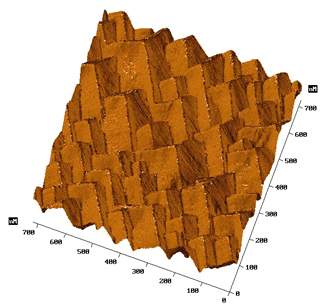
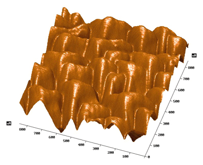
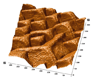
1) Multiple peaks at the apex comprising atomic scale protrusions. Every peak during scanning contributes in the tip-sample interaction. In the simplest case of a double peak apex the features on the sample surface look double in the scans (Fig. 3, d). Absence of this defect is especially crucial when measuring single macromolecules.
2) Blunt apex. This results in lowering of resolution power. The sharpness of the apex tends to decrease during consecutive contact mode scans of the sample surface (Fig. 3, a,b,c).
3) Non-spherical apex. Results in geometry distortion of sample features.
 |
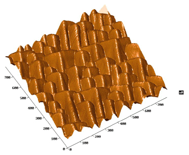 |
| (a) 700 x 700 x 20 nm | (b) 700 x 700 x 16 nm |
 |
 |
| (c) 800 x 800 x 12 nm | (d) 400 x 400 x 16 nm |
Fig. 3. Imaging of sharp edges of CdF2 films grown in <111> orientation. a, b, c) Decreasing of AFM tip sharpness in the set. d) Double tip artifact. Image courtesy of Prof. Sergey Gastev, St. Petersburg |
|
As a matter of fact, the yield of AFM cantilevers with "good" AFM tips is occasionally not very close to 100% due to defects of one type or another including the most common mentioned above. Thus, development of a simple AFM tip shape characterization technique is quite desirable. Moreover, scanning probe techniques are utilized as the means of choice for critical dimension metrology (CDM) applications [837, 1608, 1612] increasingly in recent years, and the AFM tip shape geometry becomes a crucial factor of success.
Problem of tip-sample convolution. Methods of AFM tip characterization.
Achieving the best possible resolution will always remain the outmost goal for many SPM studies. There are, though, some technical challenges to be overcome as well as fundamental limitations on the way to high resolution.
One of the technical issues that has to be considered is the imperfect geometry and finite size of the AFM tip. The best approximation to the ideal AFM tip geometry (omitting various natural disturbing factors like thermal noise) is believed to be a carbon nanotube of several nanometers in diameter, several micrometers long and with a single atom at the sharp conical apex. Most of the commercial AFM probes are too far from this ideal case. In general, a conventional AFM tip is unable to penetrate high aspect ratio structures, to touch every point on the sample surface and to profile exactly surfaces with complex topography. In this way, the finite size of the AFM tip and its imperfectness contribute significantly to distortion of images.
There are also some physical restrictions in achieving subnanometer resolution besides technical issues. Due to the long-range nature of van der Waals forces acting between AFM tip and sample, resulting force is determined by the mean interaction of a large number of atoms from both the AFM tip and the sample surface especially when the features are comparable in size with AFM tip apex. Therefore, the features of the sample surface become diluted by this interaction of collective nature.
Thus, actually the image is a complex convolution of the AFM tip and the surface shapes. This convolution is unavoidable but there are ways to reconstruct a rather accurate image from the diluted one using special mathematical methods.
The earliest attempts to formulate the task mathematically date from papers of Reiss et al. [1633] and Keller [1634]. Their works have become the basis for several similar methods of deconvolution where some simple particular geometries, e.g. spheres or parabolas are considered. These methods require intensive computation and evaluation of numerical derivatives and, therefore are comlicated enough for practical implementation.
Another approach to solve the problem of deconvolution relies on mathematical morphology. This approach has been proposed and developed by many authors [1637] beginning from works of Gallarda and Jain [1635] and Pingali and Jain [1636]. It is applicable to general shapes (any AFM tip and sample which can be expressed as an array of heights in the usual fashion), and does not require numerical derivatives.
These methods have one point in common - it is necessary beforehand to estimate the AFM tip geometry in order to perform proper deconvolution procedure thereafter. One of the most popular methods for AFM tip shape and size determination is based on the so-called AFM tip characterizers, which are the features of well-defined geometry at the nanoscale. Characterizers may be highly ordered edges of crystal facets (SrTiO3 [1603], MgO and NaCl [1604]), nanoparticles of well-defined spherical form [1605, 1607], sputtered cones [51] or nanoparticles [27] of InP, spike-like features in hydrothermally deposited ZnO films [268], macromolecules [788, 1455] and many others [E010]. Additionally, specially designed calibration standards can also serve as AFM tip characterizers. A computer analysis of the obtained scans can help restore the AFM tip shape and at the same time deduce what kind of defect the AFM tip contains.
An alternative widely used approach for AFM tip shape determination has come to be known as "blind reconstruction". The term "blind" means that there is no need of a priory knowledge of the exact characterizer's actual geometry. Since the publication of the principles of general blind reconstruction by Villarrubia [1639] equivalent or similar methods independently are discovered later [1643, 1644]. The algorithms of blind reconstruction are published in [1645] and a speedier version is described and tested in [1646]. It is experimentally verified to work in a comparison between blind reconstruction of an AFM tip and an independent method [1647]. In other work Todd and Eppell report on the improvement of this method in respect to spatially anisotropic noise which generally takes place at the nanoscale and introduces an error in the AFM tip geometry determination [801]. The latest advances in evaluation of AFM tip performance in the blind reconstruction method can be found in the papers of Nie et al. [1654, 1656].
Another modern technique developed by S. Xu et al. [23] is called nanografting. It is based on subsequent imaging of a thiol self-assembled monolayer. The authors state that this method features simplicity, high speed and the ability to characterize the very top portion of the AFM tip. Moreover, AFM tips with multiple asperities, which are difficult to investigate using other approaches, can be easily identified and characterized via nanografting.
We would like to express special thanks to John Villarrubia from the National Institute of Standards and Technology (Gaithersburg, MD, USA) for the constructive discussion on the content of this paragraph.
Please, send all comments and suggestions concerning these pages to info@mikromasch.com.
| ID | Reference list |
| 13 | Effect of tip morphology on AFM images S.H. Ke, T. Uda, I. Stich, K. Terakura Applied Physics A: Materials Science & Processing, 72 (2001), S63-S66 |
| 17 | Forces with submolecular resolution between the probing tip and Cu-TBPP molecules on Cu(100) observed with a combined AFM/STM Ch. Loppacher, M. Bammerlin, M. Guggisberg, E. Meyer, H.-J. Guntherodt, R. Luthi, R. Schlittler, J.K. Gimzewski Applied Physics A: Materials Science & Processing, 72 (2001), S105-S108 |
| 21 | Influence of tip size on AFM roughness measurements D.L. Sedin, K.L. Rowlen Applied Surface Science, 182 (2001), 1-2, 40-48 |
| 23 | Characterization of AFM tips using nanografting S. Xu, N.A. Amro, G.-Y. Liu Applied Surface Science, 175-176 (2001), 649-655 |
| 27 | Evaluation of AFM tips using nanometer-sized structures induced by ion sputtering F. Frost, D. Hirsch, A. Schindler Applied Surface Science, 179 (2001), 1-4, 8-12 |
| 30 | Simulated nc-AFM images of Si(001) surface with nanotube tip K. Tagami, N. Sasaki, M. Tsukada Applied Surface Science, 172 (2001), 3-4, 301-306 |
| 47 | Theory for the effect of the tip-surface interaction potential on atomic resolution in forced vibration system of noncontact AFM N. Sasaki, M. Tsukada Applied Surface Science, 140 (1999), 3-4, 339-343 |
| 51 | Cones formed during sputtering of InP and their use in defining AFM tip shapes M.P. Seah, J.E. Johnstone, S.J. Spencer, P.J. Cumpson Applied Surface Science, 144-145 (1999), 151-155 |
| 78 | Functionalization of carbon nanotube AFM probes using tip-activated gases A.T. Woolley, E. Joselevich, C.M. Lieber, S.S. Wong Chemical Physics Letters, 306 (1999), 5-6, 219-225 |
| 82 | Intrinsic stress measured on ultra-thin amorphous carbon films deposited on AFM cantilevers P. Lemoine, J.F. Zhao, A. Bell, P. Maguire, J. McLaughlin Diamond and Related Materials, 10 (2001), 1, 94-98 |
| 85 | Characterization of AFM cantilevers coated with diamond-like carbon M.C. Salvadori, M.C. Fritz, C. Carraro, R. Maboudian, O.R. Monteiro, I.G. Brown Diamond and Related Materials, 10 (2001), 12, 2190-2194 |
| 132 | Sizes correction on AFM images of nanometer spherical particles De-Quan Yang, Yu-Qing Xiong, Yun Guo, Da-An Da, Wei-Gang Lu Journal of Materials Science (full set), 36 (2000), 1, pp. 263-267 |
| 153 | Multifunctional AFM/SNOM Cantilever Probes: Fabrication and Measurements M. Stopka, D. Drews, K. Mayr, M. Lacher, W. Ehrfeld, T. Kalkbrenner, M. Graf, V. Sandoghdar, J. Mlynek Microelectronic Engineering, 53 (2000), 1-4, 183-186 |
| 157 | Integrating diamond pyramids into metal cantilevers and using them as electrical AFM probes T. Hantschel, S. Slesazeck, P. Niedermann, P. Eyben, W. Vandervorst Microelectronic Engineering, 57-58 (2001), 749-754 |
| 160 | Piezoresistive sensors on AFM cantilevers with atomic resolution R. Jumpertz, O. Ohlsson, A.v.d. Hart, J. Schelten, F. Saurenbach Microelectronic Engineering, 41-42 (1998), 441-444 |
| 161 | Fabrication of Multipurpose AFM/SCM/SEP Microprobe with Integrated Piezoresistive Deflection Sensor and Isolated Conductive Tip P. Hudek, P. Grabiec, F. Shi, T. Gotszalk, I.W. Rangelow, P. Dumania Microelectronic Engineering, 41-42 (1998), 477-480 |
| 163 | 6.6 MHz silicon AFM cantilever for high-speed readout in AFM-based recording K. Itoh, H. Koyanagi, K. Etoh, S. Hosaka, A. Kikukawa Microelectronic Engineering, 46 (1999), 1-4, 109-112 |
| 164 | Tip-on-tip: a novel AFM tip configuration for the electrical characterization of semiconductor devices W. Kulisch, W. Vandervorst, T. Hantschel, T. Trenkler, A. Malave, D. Buchel, E. Oesterschulze Microelectronic Engineering, 46 (1999), 1-4, 113-116 |
| 184 | First AFM observation of thin cermet films close to the percolation threshold using a conducting tip M. Gadenne, P. Gadenne, O. Schneegans, F. Houze, P. Chretien, C. Desmarest, J. Sztern Physica B: Condensed Matter, 279 (2000), 1-3, 94-97 |
| 210 | Fabrication and characterization of cantilevers with integrated sharp tips and piezoelectric elements for actuation and detection for parallel AFM applications N.F. De Rooij, G. Schurmann, G.-A. Racine, P.-F. Indermuhle Sensors and Actuators A: Physical, 60 (1997), 1-3, 186-190 |
| 211 | Piezoresistive silicon V-AFM cantilevers for high-speed imaging A.G.R. Evans, A. Brunnschweiler, G. Ensell, Y. Su Sensors and Actuators A: Physical, 76 (1999), 1-3, 139-144 |
| 213 | AFM imaging with an xy-micropositioner with integrated tip P.-F. Indermuhle, V.P. Jaecklin, J. Brugger, C. Linder, N.F. De Rooij, M. Binggeli Sensors and Actuators A: Physical, 47 (1995), 1-3, 562-565 |
| 214 | Modular design of AFM probe with sputtered silicon tip P.A. Rasmussen, J. Thaysen, S. Bouwstra, A. Boisen Sensors and Actuators A: Physical, 92 (2001), 1-3, 96-101 |
| 220 | Structuring of mica surfaces with a vibrating AFM tip J. Kuppers, T. Schimmel, R. Kladny, V. Popp Surface Science, 401 (1998), 1, 105-111 |
| 227 | Current-dependent growth of silicon nitride lines using a conducting tip AFM D. Sarid, C.A. Peterson, R.K. Workman Surface Science, 423 (1999), 2-3, L277-L279 |
| 237 | Direct imaging of the tip shape by AFM. A. Baiker, F. Atamny Surface Science, 323 (1995), 3, l314-l318 |
| 243 | Simulation of interaction force between Si tip and Si(111)3x3-Ag surface of IET structure in noncontact AFM N. Sasaki, S. Watanabe, H. Aizawa, M. Tsukada Surface Science, 493 (2001), 1-3, 188-193 |
| 268 | Characterization of atomic force microscopy (AFM) tip shapes by scanning hydrothermally deposited ZnO thin films G.W. Bao, S.F.Y. Li Talanta, 45 (1998), 4, 751-757 |
| 270 | A tower-shaped prototypic molecule designed as an atomically sharp tip for AFM applications A.V. Rukavishnikov, M.D. Lee, A. Phadke, D.H. LaMunyo, P.A. Petukov, J.F. Keana Tetrahedron Letters, 40 (1999), 35, 6353-6356 |
| 282 | AFM for the imaging of large and steep submicroscopic features, artifacts and scraping with asymmetric cantilever tips G. Kaupp, J. Schmeyers, U. Pogodda, M. Haak, T. Marquardt, M. Plagmann Thin Solid Films, 264 (1995), 2, 205-211 |
| 332 | Application of the needle sensor for microstructure measurements and atomic force microscopy U. Grunewald, K. Bartzke, T. Antrack Thin Solid Films, 264 (1995), 2, pp. 169-171 |
| 390 | Atomic force microscopy probe with piezoresistive read-out and a highly symmetrical Wheatstone bridge arrangement J. Thaysen, A. Boisen, O. Hansen, S. Bouwstra Sensors and Actuators A: Physical, 83 (2000), 1-3, 47-53 |
| 451 | Chemical bonds studied with functionalized atomic force microscopy tips T. Han, J.M. Williams, T.P. Beebe Analytica Chimica Acta, 307 (1995), 2-3, 365-376 |
| 487 | Effect of tip sharpness on the relative contributions of attractive and repulsive forces in the phase imaging of tapping mode atomic force microscopy M.-H. Whangbo, R. Brandsch, G. Bar Surface Science, 422 (1999), 1-3, L192-L199 |
| 519 | Harmonic responses of a cantilever interacting with elastomers in tapping mode atomic force microscopy M.-H. Whangbo, G. Bar, R. Brandsch, L. Delineau Surface Science, 448 (2000), 1, L179-L187 |
| 537 | Imaging silicon by atomic force microscopy with crystallographically oriented tips F.J. Giessibl, S. Hembacher, H. Bielefeldt, J. Mannhart Applied Physics A: Materials Science & Processing, 72 (2001), 7, S15-S17 |
| 581 | Lead zirconate titanate cantilever for noncontact atomic force microscopy T. Fujii, Y. Miyahara, H. Bleuler, H. Yamada, A. Tonoli, S. Watanabe, S. Carabelli Applied Surface Science, 140 (1999), 3-4, 428-431 |
| 602 | Micromachining of diamond probes for atomic force microscopy applications K. Unno, T. Shibata, E. Makino Sensors and Actuators A: Physical, 88 (2001), 3, 247-255 |
| 642 | Non-contact atomic force microscopy of an antiferromagnetic NiO(100) surface using a ferromagnetic tip H. Hosoi, M. Kimura, K. Hayakawa, K. Sueoka, K. Mukasa Applied Physics A: Materials Science & Processing, 72 (2001), 7, S23-S26 |
| 698 | Simulation of atomic force microscopy image variations due to tip apex size: Appearance of half spots M. Komiyama, K. Tazawa, K. Tsujimichi, A. Hirotani, M. Kubo, A. Miyamoto Thin Solid Films, 281-282 (1996), 1-2, 580-583 |
| 756 | The determination of the elastic modulus of microcantilever beams using atomic force microscopy B. T. Comella, M. R. Scanlon Journal of Materials Science (full set), 35 (2000), 3, 567-572 |
| 788 | Calibration of atomic force microscope tips using biomolecules Thundat, T., Zheng, X. -Y., Sharp, S. L., Allison, D. P., Warmack, R. J., Joy, D. C. and Ferrell, T. L. Scanning Microsc. 6 (1992), 903-910 |
| 801 | A method to improve the quantitative analysis of SFM images at the nanoscale B.A. Todd, S.J. Eppell Surface Science, 491 (2001), 3, 473-483 |
| 818 | Carbon nanotubes as tips in non-contact SFM V. Barwich, M. Bammerlin, A. Baratoff, R. Bennewitz, M. Guggisberg, C. Loppacher, O. Pfeiffer, E. Meyer, H.-J. Guntherodt, J.-P. Salvetat, J.-M. Bonard, L. Forro Applied Surface Science, 157 (2000), 4, 269-273 |
| 837 | Intercomparison of SEM, AFM, and Electrical Linewidths J. S. Villarrubia, R. Dixson, S. Jones, J. R. Lowney, M. T. Postek, R. A. Allen, and M. W. Cresswell Metrology, Inspection, and Process Control for Microlithography XIII, Proc. SPIE 3677 (1999), pp. 587-598 . |
| 859 | Lateral stiffness: A new nanomechanical measurement for the determination of shear strengths with friction force microscopy R. W. Carpick, D. F. Ogletree and M. Salmeron Applied Physics Letters 70 (1997), 1548 |
| 860 | Investigating the effects of silicon tip contamination in noncontact scanning force microscopy (SFM) A.S. Foster, P.V. Sushko, A.L. Shluger, L.N. Kantorovich Applied Surface Science, 144-145 (1999), 608-612 |
| 870 | Lithographically defined polymer tips for quartz tuning fork based scanning force microscopes T. Akiyama, U. Staufer, N.F. de Rooij, L. Howald, L. Scandella Microelectronic Engineering, 57-58 (2001), 769-773 |
| 873 | Magnetically refined tips for Scanning Force Microscopy R. Jumpertz, P. Leinenbach, A.W.A. van der Hart, J. Schelten Microelectronic Engineering, 35 (1997), 1-4, 325-328 |
| 878 | Micromachined Si3N4-Tip on Cantilever for Parallel SFM and NSOM Applications S.S. Choi, M.Y. Jung, I.W. Lyo Microelectronic Engineering, 46 (1999), 1-4, 427-430 |
| 886 | Non-destructive imaging of delicate polymer surfaces using scanning force microscopy tips modified with hydrophobic self-assembled monolayers G.J. Leggett, B.D. Beake Polymer, 40 (1999), 21, 5973-5976 |
| 921 | Self-excited force-sensing microcantilevers with piezoelectric thin films for dynamic scanning force microscopy T. Itoh, T. Suga Sensors and Actuators A: Physical, 54 (1996), 1-3, 477-481 |
| 922 | Self-excited piezoelectric PZT microcantilevers for dynamic SFM-with inherent sensing and actuating capabilities T. Itoh, T. Suga, C. Lee Sensors and Actuators A: Physical, 72 (1999), 2, 179-188 |
| 933 | Study of tip-sample interaction in scanning force microscopy M. Luna, J. Colchero, J. Gomez-Herrero, A.M. Baro Applied Surface Science, 157 (2000), 4, 285-289 |
| 943 | Tapping-mode scanning force microscopy: Metallic tips and samples D. Sarid Computational Materials Science, 5 (1996), 4, 291-297 |
| 972 | Studies of vibrating atomic force microscope cantilevers in liquid Schaeffer T.E., Cleveland J.P., Ohnesorge F.M., Walters D.A., Hansma P.K. J. Appl. Phys. 80 (1996), 3622-3627. |
| 974 | Investigation of the image contrast of tapping-mode atomic force microscopy using protein-modified cantilever tips You H.X., Yu L. Biophys. J. 73 (1997), 3299-3308. |
| 1007 | Application of commercially available cantilevers in tuning fork Scanning Probe Microscopy (SPM) studies S. Rozhok, V. Chandrasekhar Solid State Communications, 121 (2002), 12, 683-686 |
| 1010 | Artifacts in SPM measurements of thin films and coatings T.G. Lenihan, A.P. Malshe, W.D. Brown, L.W. Schaper Thin Solid Films, 270 (1995), 1-2, 356-361 |
| 1022 | Fabrication of integrated diamond cantilevers with tips for SPM applications W. Kulisch, A. Malave, W. Scholz, C. Mihalcea, E. Oesterschulze, G. Lippold Diamond and Related Materials, 6 (1997), 5-7, 906-911 |
| 1025 | In situ scanning probe microscopy and new perspectives in analytical chemistry A.G. Hansen, A. Boisen, J.-D. Zhang, J.U. Nielsen, J.E.T. Andersen, J. Ulstrup, H. Jensenius, E.P. Friis, Q. Chi Trends in Analytical Chemistry, 18 (1999), 11, 665-674 |
| 1026 | Indirect tip fabrication for Scanning Probe Microscopy J.P. Rasmussen, O. Hansen, S. Bouwstra, A. Boisen Microelectronic Engineering, 30 (1996), 1-4, 579-582 |
| 1033 | Melnikov-Based Dynamical Analysis of Microcantilevers in Scanning Probe Microscopy M. Ashhab, M. V. Salapaka, M. Dahleh, I. Mezic Nonlinear Dynamics, 20 (1999), 3, 197-220 |
| 1065 | Spring constants of composite ceramic/gold cantilevers for scanning probe microscopy J.L. Hazel, V.V. Tsukruk Thin Solid Films, 339 (1999), 1-2, 249-257 |
| 1105 | Cantilever vibration control by electrostatic actuation for magnetic force microscopy M.J. Cunningham, D.F.L. Jenkins, M.A.H. Khalid Sensors and Actuators A: Physical, 63 (1997), 2, 125-128 |
| 1110 | Description of magnetic force microscopy by three-dimensional tip Green's function for sample magnetic charges H. Saito, S. Ishio, J. Chen Journal of Magnetism and Magnetic Materials, 191 (1999), 1-2, 153-161 |
| 1111 | Development of high coercivity magnetic force microscopy tips S.H. Liou, Y.D. Yao Journal of Magnetism and Magnetic Materials, 190 (1998), 1-2, 130-134 |
| 1117 | Fabrication and characterization of advanced probes for magnetic force microscopy U. Hartmann, J. Schelten, P. Leinenbach, U. Memmert Applied Surface Science, 144-145 (1999), 492-496 |
| 1122 | Interactions between soft magnetic samples and MFM tips S.L. Tomlinson, A.N. Farley, S.R. Hoon, M.S. Valera Journal of Magnetism and Magnetic Materials, 157-158 (1996), 557-558 |
| 1123 | Interpretation of low-coercivity tip response in MFM imaging R. Street, D.L. Bradbury, L. Folks Journal of Magnetism and Magnetic Materials, 177-181 (1998), 2002, 980-981 |
| 1126 | Investigation of the response of a new amorphous ferromagnetic MFM tip coating with an established sample and a prototype device G.P. Heydon, W.M. Rainforth, M.R.J. Gibbs, H.A. Davies, J.E.L. Bishop, J.W. Tucker, S. Huo, G. Pan, D.J. Mapps, W.W. Clegg Journal of Magnetism and Magnetic Materials, 214 (2000), 3, 225-233 |
| 1176 | Preparation and characterisation of a new amorphous tip coating for application in magnetic force microscopy H.A. Davies, S. McVitie, M.R.J. Gibbs, R.P. Ferrier, W.M. Rainforth, J. Scott, G.P. Heydon, J.W. Tucker, J.E.L. Bishop Journal of Magnetism and Magnetic Materials, 205 (1999), 2-3, 131-135 |
| 1181 | Rapid biochemical detection and differentiation with magnetic force microscope cantilever arrays R.G. Rudnitsky, E.M. Chow, T.W. Kenny Sensors and Actuators A: Physical, 83 (2000), 1-3, 256-262 |
| 1205 | Method for the calibration of atomic-force microscope cantilevers J.E. Sader, I. Larson, P. Mulvaney and L.R. White Rev. Sci. Instrum., 66 (1995) 3789-3798 |
| 1206 | Calibration of rectangular atomic force microscope cantilevers J.E. Sader, J.W.M. Chon and P. Mulvaney Rev. Sci. Instrum., 70 (1999) 3967-3969 |
| 1210 | Quality Factors in Micron- and Submicron-Thick Cantilevers K. Y. Yasumura, T. D. Stowe, E. M. Chow, T. Pfafman, T. W. Kenny, B. C. Stipe and D. Rugar Journal of Microelectromechanical Systems, 9 (2000) 1, pp. 117-125 |
| 1211 | Functionalization of scanning force microscopy cantilevers via galvanic displacement technique M. C. Fritz, C. Carraro and R. Maboudian Tribology Letters, 11 (2001), 3-4, 171-175 |
| 1218 | Lateral, normal, and longitudinal spring constants of atomic force microscopy cantilevers Neumeister, J. M. and W. A. Ducker Rev. Sci. Instrum., 65 (1994), 8, 2527-2531 |
| 1281 | Whisker probes Givargizov E.I., Stepanova A.N.,Obolenskaya L.N.,Mashkova E.S., Molchanov V.A.,Givargizov M.E., Rangelow I. Ultramicroscopy, 82 (2000), p. 57-61 |
| 1300 | A new calibration method of the lateral contact stiffness and lateral force using modulated lateral force microscopy O. Pietrement, J.L. Beaudoin, M. Troyon Tribology Letters, 7 (1999), 4, 213-220 |
| 1308 | Lateral force microscopy - A quantitative approach C.T. Gibson, G.S. Watson, S. Myhra Wear, 213 (1997), 1-2, pp. 72-79 |
| 1325 | Carbon-nanotube tips for scanning probe microscopy: Preparation by a controlled process and observation of deoxyribonucleic acid H.Nishijima, S.Kamo, S.Akita, Y.Nakayama, K.I.Hohmura, S.H.Yoshimura, K.Takeyasu Appl. Phys. Lett. 74 (1999), 26, pp. 4061-4063 |
| 1328 | Preparation of platinum iridium scanning probe microscopy tips A. H. Sorensen, U. Hvid, M. W. Mortensen, K. A. Morch Rev. Sci. Instrum. 70 (1999) 7, pp. 3059-3067 |
| 1336 | Ultrasharp diamond-coated silicon tips for scanning-probe devices E. I. Givargizov, A.N. Stepanova, E. S. Mashkova, V. A. Molchanov, F. Shi, P. Hudek and I. W. Rangelow Microelectronic Engineering 41/42 (1998) 499-502 |
| 1341 | Test structure for SPM tip shape deconvolution V. Bykov, A. Gologanov, V. Shevyakov Appl. Phys. A 66 (1998), 499-502 |
| 1358 | Sensitivity of vibration modes of atomic force microscope cantilevers in continuous surface contact Win-Jin Chang Nanotechnology 13 (2002) 510-514 |
| 1376 | Optical interference artifacts in contact atomic force microscopy images A. Mendez-Vilas, M.L. Gonzalez-Martin and M.J. Nuevo Ultramicroscopy, Vol. 92 (3-4) (2002) pp. 243-250 |
| 1378 | A complementary-metal-oxide-semiconductor-field-effect-transistor-compatible atomic force microscopy tip fabrication process and integrated atomic force microscopy cantilevers fabricated with this process Mizuki Ono, Dirk Lange, Oliver Brand, Christoph Hagleitner and Henry Baltes Ultramicroscopy, Vol. 91 (1-4) (2002) pp. 9-20 |
| 1379 | Mapping of lateral vibration of the tip in atomic force microscopy at the torsional resonance of the cantilever Takayoshi Kawagishi, Atsushi Kato, Yasuo Hoshi and Hideki Kawakatsu Ultramicroscopy, Vol. 91 (1-4) (2002) pp. 37-48 |
| 1380 | Scanning probe microscopy installed with nanotube probes and nanotube tweezers Yoshikazu Nakayama Ultramicroscopy, Vol. 91 (1-4) (2002) pp. 49-56 |
| 1381 | Performance of the carbon nano-tube assembled tip for surface shape characterization M. Yasutake, Y. Shirakawabe, T. Okawa, S. Mizooka and Y. Nakayama Ultramicroscopy, Vol. 91 (1-4) (2002) pp. 57-62 |
| 1382 | Self-sensing piezoresistive cantilever and its magnetic force microscopy applications Hiroshi Takahashi, Kazunori Ando and Yoshiharu Shirakawabe Ultramicroscopy, Vol. 91 (1-4) (2002) pp. 63-72 |
| 1437 | Atomic Force Microscopy Cantilevers for Sensitive Lateral Force Detection M. Kageshima, H. Ogiso, S. Nakano, M. A. Lantzand and H. Tokumoto Jpn. J. Appl. Phys., 38 (1999) 3958-3961 |
| 1441 | Electrochemically etched nickel tips for spin polarized scanning tunneling microscopy Cavallini M. and Biscarini F. Rev. Sci. Instrum., 71 (2000), 12, pp. 4457-4460 |
| 1442 | Silicon nitride Cantilevers with Oxidation-Sharpened Silicon Tips for Atomic Force Microscopy R. J. Grow, S. C. Minne, S. R. Manalis and C. F. Quate Journal of Microelectromechanical Systems, 11 (2002) 4, pp. 317-321 |
| 1445 | WS2 nanotubes as tips in scanning probe microscopy A.Rothschild, S.R.Cohen, R.Tenne Appl. Phys. Lett. 75 (1999), 25, pp. 4025-4027 |
| 1455 | AFM structural study of the molecular chaperone GroEL and its two-dimensional crystals: an ideal "living" calibration sample F. Valle, J.A. DeRose, G. Dietler, M. Kawe, A. Plückthun and G. Semenza Ultramicroscopy, Vol. 93 (1) (2002) pp. 83-89 |
| 1456 | Atomic force microscopy using single-wall C nanotube probes E. S. Snow, P. M. Campbell, and J. P. Novak J. Vac. Sci. Tech. B 20, 2002, 822 |
| 1464 | Terabit-per-square-inch data storage with the atomic force microscope E. B. Cooper, S. R. Manalis, H. Fang, H. Dai, K. Matsumoto, S. C. Minne, T. Hunt, and C. F. Quate Appl. Phys. Lett. 75 (1999), 22, 3566-3568 |
| 1578 | Fast imaging and fast force spectroscopy of single biopolymers with a new atomic force microscope designed for small cantilevers Viani, M. B., T. E. Schaeffer, G. T. Paloczi, L. I. Pietrasanta, B. L. Smith, J. B. Thompson, M. Richter, M. Rief, H. E. Gaub, K. W. Plaxco, A. N. Cleland, H. G. Hansma, and P. K. Hansma. Rev. Sci. Instrum. 70 (1999), 4300-4303. |
| 1603 | Mesoscopic Calibration of an Atomic Force Microscope S.S. Sheiko, M. Möller, E.M.C.M. Reuvekamp and H.W. Zandbergen Ultramicroscopy 53 (1994) 371-380 |
| 1604 | Determining the form of atomic force microscope tips P. Siedle, H-J. Butt. E.Bamberg, D.N. Wang, W. Kuhlbrand, J. Zach and M. Haider Int. Phys. Conf. Ser. 130 (1993) 361 |
| 1605 | Calibration of the scanning (atomic) force microscope with gold particles S.Xu and M.F.Arnsdorf J. Microsc. 173 (1994) 199 |
| 1606 | CVD diamond probes for nanotechnology P. Niedermann, W. Hanni, D. Morel, A. Perret, N. Skinner, P.-F. Indermuhle, N.-F. de Rooij , P.-A. Buffat Applied Physics A: Materials Science & Processing, 66 (1998), 7, S31-S34 |
| 1607 | Tip Characterization from AFM Images of Nanometric Spherical Particles Ramirez-Aguilar, K. A.; Rowlen, K. L. Langmuir, 14 (1998), 2562-2566 |
| 1608 | Tip shape effects in scanning probe metrology R. Cottle Proc. SPIE, Vol. 4562 (2002), p. 247-255 |
| 1609 | Fabrication of monolithic diamond probes for scanning probe microscopy applications Scholz, Wenzel; Albert, D.; Malave, A.; Werner, Stephfan; Mihalcea, Christopher; Kulisch, W.;Oesterschulze, Egbert Proc. SPIE Vol. 3009 (1997), p. 61-71 |
| 1610 | Sharpened carbon nanotube probes Moloni, Katerina; Lal, Amit; Lagally, Max G. Proc. SPIE Vol. 4098 (2000), p. 76-83 |
| 1611 | Electric force microscopy with a single carbon nanotube tip Dagata, John A.; Chien, F. S.; Gwo, S.; Morimoto, K.; Inoue, Takahito; Itoh, J.; Yokoyama, Hiroshi Proc. SPIE Vol. 4344 (2001) p. 58-71 |
| 1612 | Using carbon nanotube cantilevers in scanning probe metrology R. Schlaf, Y. Emirov, J.A. Bieber, A. Sikder, J. Kohlscheen, D.A. Walters, M.R. Islam, B. Metha, Z. F. Ren, T.L. Shofner, B.B. Rossie, M.W. Cresswell Proc. SPIE Vol 4689 (2002), (in print) |
| 1613 | Carbon nanotubes as probes for atomic force microscopy R. M. D. Stevens, N. A. Frederick, B. L. Smith, D. E. Morse, G. D. Stucky and P. K. Hansma Nanotechnology 11 (2000), 1-5 |
| 1614 | Carbon nanotube tips - high-resolution probes for imaging biological systems S.S. Wong, J.D. Harper, P.T. Lansbury Jr., C.M. Lieber J. Am. Chem. Soc. 120, 1998, 603-604 |
| 1615 | Single-walled carbon nanostructure probes for high-resolution nanostructure imaging S.S. Wong, A.T. Woolley, T.W. Odom, J.-L. Huang, P. Kim, D.V. Vezenov, C.M. Lieber Appl. Phys. Lett. 73, 1998, 3465-3467 |
| 1616 | Growth of nanotubes for probe microscopy tips J. H. Hafner, C. L. Cheung, and C. M. Lieber Nature, 398 (1999) N6730, 761 |
| 1617 | Nanotube as Nanoprobes in Scanning Probe Microscopy Dai, H.; Hafner, J. H.; Rinzler, A. G.; Colbert, D. T.; Smalley, R. E. Nature, 384 (1996), 147 |
| 1618 | Structural and Functional Imaging with Nanotube AFM probes Hafner, J. H.; Cheung, C. L.; Woolley, A. T.; Lieber, C. M. Progress in Biophysics and Molcular Biology, 77 (2001), pp. 73 |
| 1619 | Exploiting the properties of carbon nanotubes for nanolithography H. Dai, N. Franklin, and J. Han Appl. Phys. Lett. 73 (1998), 1508-1510 |
| 1620 | High-Yield Assembly of Individual Single-Walled Carbon Nanotube Tips for Scanning Probe Microscopies Jason H. Hafner, Chin-Li Cheung, Tjerk H. Oosterkamp, and Charles M. Lieber J. Phys. Chem. B 105 (2001) 4, 743-746 |
| 1621 | Calibration of the Torsional Spring Constant and the Lateral Photodiode Response of Friction Force Microscopes A. Feiler, P. Attard, I. Larson Rev. Sci. Instrum. 71 (2000), 2746-2750 |
| 1622 | Stability of thiol-immobilized DNA on microcantilever sensors K.A. Stevenson, A. Mehta, K.M. Hansen and T.G. Thundat Proc. ESC 201 Meeting - Philadelphia, Pennsylvania, May 12-17 (2002) |
| 1623 | In situ detection of calcium ions with chemically modified microcantilevers H.-F. Ji and T. G. Thundat Biosensors & Bioelectronics, 2002, 17, 337-343 |
| 1624 | Ultrasensitive Detection of Trace CrO42- Using a Microcantilever sensors H.-F. Ji, T. Thundat, R. Dabestani, G. M. Brown, P. F. Britt, and P. Bonnesson Anal. Chem. 2001, 73(7), 1572-1576 |
| 1625 | Nanomechanical Signatures of Biomolecular Recognition and Interactions G. Wu, H. -F. Ji, K. Hansen, T. Thundat, R. Datar, R. Cote, M. F. Hagan, A. K. Chakraborty, and A. Majumdar Proc. Natl. Acad. Sci. 2001, 98, 1560-1564 |
| 1626 | Cantilever-based optical deflection assay for discrimination of DNA single nucleotide mismatches K. M. Hansen, H.-F. Ji, G. Wu, R. Datar, R. Cote, A. Majumdar, T. Thundat Anal. Chem., 2001, 73(7), 1567-1571 |
| 1627 | Detection of pH variation Using Modified Microcantilever Sensors H.-F. Ji, K. M. Hansen, Z. Hu, T. Thundat Sensors and Actuators B: Chemical, 72 (2001), 233-238 |
| 1628 | A Novel Self-Assembled Monolayer Coated Microcantilever for Low Level Cesium Detection H. F. Ji, R. Dabestani, E. Finot, T. Thundat, G. M. Brown and P. F. Britt Chem. Commun., 2000, 457 |
| 1629 | Highly Selective Microcantilever Sensor for Cesium Ion Detection T. Thundat, E. Finot, H.-F. Ji, R. Dabestani, P.F. Britt, P. V. Bonnesen, G. M. Brown, R. J. Warmack Proc. Electrochem. Soc., 1999, 99-23, 314-319 |
| 1630 | In-situ Detection of DNA hybridization using Browninan Motion of Microcantilevers H.-F. Ji, K. M. Hansen, T. Thundat, G. Wu, A. Majumdar, R. Datar, and R. Cote Submitted to Anal. Chem. |
| 1631 | Ultrasensitive Detection of Hg2+ Using Microcantilever Sensors X. Xu, T. Thundat, G. M. Brown, and H. F. Ji Submitted for publication. |
| 1633 | Scanning tunneling microscopy on rough surfaces-deconvolution of constant current images G. Reiss, F. Schneider, J. Vancea, and H. Hoffmann Appl. Phys. Lett. 57 (1990), 867 |
| 1634 | Reconstruction of STM and AFM images distorted by finite-size tips D. Keller Surf. Sci. 253 (1991), 353 |
| 1635 | Computational model of the imaging process in scanning-x microscopy H. Gallarda and R. Jain Proceedings of Conference on Integrated Circuit Metrology, Inspection, and Process Control, V, SPIE Vol. 1464 (1991), 459 |
| 1636 | Restoration of scanning probe microscope images G. S. Pingali and R. Jain Proceedings IEEE Workshop on Applications of Computer Vision, (1992) pp. 282-289 |
| 1637 | Envelope reconstruction of probe microscope images D. J. Keller and F. S. Franke Surf. Sci. 294 (1993), 409 |
| 1638 | Atomic-force microscopy probe tip visualization and improvement of images using a simple deconvolution procedure P. Markiewicz and M. C. Goh Langmuir 10 (1994), 5 |
| 1639 | Morphological estimation of tip geometry for scanned probe microscopy J. S. Villarrubia Surf. Sci. 321 (1994), 287 |
| 1640 | A mathematical morphology approach to image-formation and image-restoreation in scanning tunneling and atomic-force microscopies N. Bonnet, S. Dongmo, P. Vautrot, and M. Troyon Microsc. Microanal. Microstruct. 5 (1994), 477 |
| 1641 | Morphological restoration of atomic-force microscopy images D. L. Wilson, K. S. Kump, S. J. Eppell, and R. E. Marchant Langmuir 11 (1995), 265 |
| 1642 | Scanned probe microscope tip characterization without calibrated tip characterizers J. S. Villarrubia J. Vac. Sci. Technol. B. 14 (1996), 1518 |
| 1643 | Blind restoration method of scanning tunneling and atomic force microscopy images S. Dongmo, M. Troyon, P. Vautrot, E. Delain, and N. Bonnet J. Vac. Sci. Technol. B 14 (1996), 1552 |
| 1644 | Blind reconstruction of scanning probe image data P. M. Williams, K. M. Shakesheff, M. C. Davies, D. E. Jackson, C. J. Roberts, and S. J. B. Tendler J. Vac. Sci. Technol. B 14 (1996), 1557 |
| 1645 | Algorithms for scanned probe microscope image simulation, surface reconstruction, and tip estimation J. S. Villarrubia J. Res. Natl. Inst. Stand. Technol. 102 (1997), 4, 425-454 |
| 1646 | A strategy for faster blind reconstruction of tip geometry for scanned probe microscopy J. S. Villarrubia Metrology, Inspection, and Process Control for Microlithography XII, Proceedings of SPIE Vol. 3332 (1998), 10 |
| 1647 | Experimental Test of Blind Tip Reconstruction for Scanning Probe Microscopy S. Dongmo, J. S. Villarrubia, S. N. Jones, T. B. Renegar, M. T. Postek, and J. F. Song Ultramicroscopy 85 (2000) 3, pp. 141-153 |
| 1649 | Micromachined silicon cantilever beams for thin-film stress measurement G.F. Cardinale, D.G. Howitt, W.M. Clift, K.F. McCarty, D.L. Medlin, P.B.Mirkarimi, N.R. Moody Thin Solid Films 287 (1996), 214-219 |
| 1246 | Frequency shifts of cantilevers vibrating in various media Stefan Weigert, Markus Dreier and Martin Hegner Appl. Phys. Lett. 69 (1996) 19, pp. 2834-2836 |
| 1247 | Carbon nanotube-modified cantilevers for improved spatial resolution in electrostatic force microscopy S. B. Arnason, A. G. Rinzler, Q. Hudspeth, and A. F. Hebard Appl. Phys. Lett. 75 (1999), 18, 2842-2844 |
| 1266 | Evaluating probes for "electrical" atomic force microscopy T. Trenkler, T. Hantschel, R. Stephenson, P. De Wolf, W. Vandervorst, L. Hellemans, A. Malave, D. Buchel, E. Oesterschulze, W. Kulisch, P. Niedermann, T. Sulzbach, and O. Ohlsson J. Vac. Sci. Technol., B18 (2000), 1, pp. 418-427 |
| 1286 | Frequency response of cantilever beams immersed in viscous fluids with applications to the atomic force microscope John Elie Sader J. Appl. Phys. 84 (1998) 1, pp. 64-76 |
| 1654 | Use of biaxially-oriented polypropylene film for evaluating and cleaning contaminated atomic force microscopy probe tips: an application to blind tip reconstruction H.-Y. Nie, M.J. Walzak and N.S. McIntyre Rev. Sci. Instrum., 73 (2002), pp. 3831-3836 |
| 1656 | A simple and effective method of evaluating atomic force microscopy tip performance H.-Y. Nie and N.S. McIntyre Langmuir 17 (2001), pp. 432-436 |
| 1687 | Chemically-Specific Probes for the Atomic Force Microscope G. U. Lee, L. A. Chrisey, C. E. O'ferral, D. E. Pilloff, N. H. Turner, and R. J. Colton Israel J. Chem. 36 (1996), pp. 81-87 |
| 1998 | Cantilevers and tips for atomic force microscopy M. Tortonese IEEE Eng Med Biol Mag, 16 (1997) 2, 28-33 |
| 1827 | Growth of tungsten carbide nano-needle and its application as a scanning tunnelling microscope tip T. Arie, S. Akita, and Y. Nakayama J. Phys. D: Appl. Phys., 31 (1998) L49-51 |
| 1878 | AFM tips: how sharp are they? S. Sheng, D. M. Czajkowsky, Z. Shao J. Microsc., 196 (1999) 1, 1-5 |
| 1824 | Carbon nanotube tips for a scanning probe microscope: their fabrication and properties S. Akita, H. Nishijima, Y. Nakayama, F. Tokumasu, and K.Takeyasu J. Phys. D: Appl. Phys., 32 (1999) 9, 1044-1048 |
| 2357 | Quality assessment of atomic force microscopy probes by scanning electron microscopy: correlation of tip structure with rendered images D. J. Taatjes, A. S. Quinn, M. R. Lewis, E. G. Bovill Microsc. Res. Tech., 44 (1999) 5, 312-326 |
| 2380 | Scanning electron microscopy studies of protein-functionalized atomic force microscopy cantilever tips M. Micic, A. Chen, R. M. Leblanc, V. T. Moy Scanning, 21 (1999) 6, 394-397 |
| 1862 | Adhesion artefacts in atomic force microscopy imaging J. I. Paredes, A. Martinez-Alonso, J. M. Tascon J. Microsc., 200 (2000) 2, 109-113 |
| 1823 | Atomic force microscopy of single-walled carbon nanotubes using carbon nanotube tip N. Choi, T. Uchihashi, H. Nishijima, T. Ishida, W. Mizutani, S. Akita, Y. Nakayama, M. Ishikawa and H. Tokumoto Jpn. J. Appl. Phys., 39 (2000) 6B, 3707-3710 |
| 1825 | Carbon-nanotube probe equipped magnetic force microscope T. Arie, H. Nishijima, S. Akita and Y. Nakayama J. Vac. Sci. Technol., B18 (2000) 1, 104-106 |
| 2047 | Comprehensive surface analysis of hydrophobically functionalized SFM tips R. Luginbuhl, A. Szuchmacher, M. D. Garrison, J. B. Lhoest, R. M. Overney, B. D. Ratner Ultramicroscopy, 82 (2000) 1-4, 171-179 |
| 2143 | Force Calibration in Lateral Force Microscopy R. G. Cain, S. Biggs, N. W. Page J. Colloid. Interface. Sci., 227 (2000) 1, 55-65 |
| 1829 | Influence of stiffness of carbon-nanotube probes in atomic force microscopy S. Akita, H. Nishijima and Y. Nakayama J. Phys. D: Appl. Phys., 33 (2000) 2673-2677 |
| 2281 | Microfabrication of a combined AFM-SNOM sensor G. Schurmann, W. Noell, U. Staufer, N. F. de Rooij Ultramicroscopy, 82 (2000) 1-4, 33-38 |
| 1831 | Microprocess for fabricating carbon-nanotube probes of a scanning probe microscope Y. Nakayama, H. Nishijima, S. Akita, K. I. Hohmura, S. H. Yoshimura and K. Takeyasu J. Vac. Sci. Technol., B18 (2000) 2, 661-664 |
| 2340 | Piezoresistive sensors for scanning probe microscopy T. Gotszalk, P. Grabiec, I. W. Rangelow Ultramicroscopy, 82 (2000) 1-4, 39-48 |
| 2200 | Implementation of self-sensing SPM cantilevers for nano-force measurement in microrobotics S. Fahlbusch, S. Fatikow Ultramicroscopy, 86 (2001) 1-2, 181-190 |
| 2217 | Integrating an ultramicroelectrode in an AFM cantilever: combined technology for enhanced information C. Kranz, G. Friedbacher, B. Mizaikoff, A. Lugstein, J. Smoliner, E. Bertagnolli Anal. Chem., 73 (2001) 11, 2491-2500 |
| 2291 | Modeling of cylindrically tapered cantilevers for transverse dynamic force microscopy (TDFM) M. Antognozzi, D. R. Binger, A. D. Humphris, P. J. James, M. J. Miles Ultramicroscopy, 86 (2001) 1-2, 223-232 |
| 1835 | Quantitative Analysis of the Magnetic Properties of a Carbon Nanotube Probe in Magnetic Force Microscopy T. Arie, N. Yoshida, S. Akita and Y. Nakayama J. Phys. D: Appl. Phys., 34 (2001) L43-L45 |
| 1836 | Reduction of Long-range Interactions using Carbon Nanotube Probes in Biological Systems Y. Maeda, H. Nishijima, S. Akita, T. Matsumoto, Y. Nakayama and T. Kawai Jpn. J. Appl. Phys., 40 (2001) 1425-1428 |
| 2594 | Focused ion beam as tool for atomic force microscope (AFM) probes sculpturing Menozzi C., L. Calabri, P. Facci, P. Pingue , F. Dinelli and P. Baschieri J. Phys.: Conf. Ser. 126 (2008) 012070 |
| 2506 | Thermomechanical noise of a free v-shaped cantilever for atomic-force microscopy R. W. Stark, T. Drobek, W. M. Heckl Ultramicroscopy, 86 (2001) 1-2, 207-215 |
| 2622 | Susceptibility of atomic force microscope cantilevers to lateral forces J.E. Sader Rev. Sci. Instrum., 74 (2003) 4, 2438-2443 |
| 2626 | Accurate analytical measurements in the atomic force microscope: a microfabricated spring constant standard potentially traceable to the SI Peter J. Cumpson and John Hedley Nanotechnology, 14 (2003) 1279-1288 |
| 2641 | Scanning Force Microscopy - Calibrative Procedures for "Best Practice" C. T. Gibson, G. S. Watson, S. Myhra Scanning, 19 (1997) 564-581 |
| 2704 | Nanometer-scale scanning sensors fabricated using stencil lithography A. R. Champagne, A. J. Couture, F. Kuemmeth, and D. C. Ralph Appl. Phys. Lett., 82 (2003) 7, 1111-1113 |
| 2800 | E2382-04 Guide to Scanner and Tip Related Artifacts in Scanning Tunneling Microscopy and Atomic Force Microscopy ASTM Annual Books of Standards, vol. 03.06 (2004) |
| 2801 | E1813-96 Standard Practice for Measuring and Reporting Probe Tip Shape in Scanning Probe Microscopy ASTM Annual Books of Standards, vol. 03.06 (2002) |
| E008 | https://web.mit.edu/cortiz/www/spring.html |
| E009 | Facile Convergent Route to Molecular Caltrops Yao Y., Tour J.M. J. Org. Chem., 1999, 64, 1968-1971 |
| E010 | https://www.weizmann.ac.il/surflab/peter/standard/ |
| E011 | https://www.surface-tec.com/pdf_files/cantilever.PDF |